thinfilm
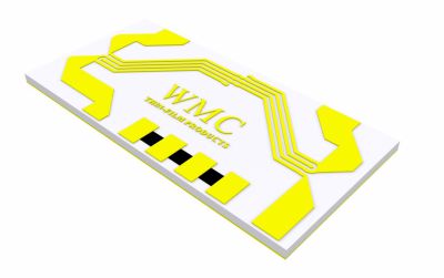


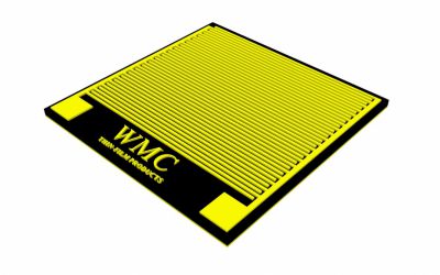
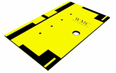
Substrate thickness: 0.002~0.004in
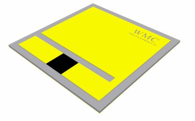
WMC THIN-FILM PRODUCTS
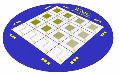
Thin film ceramic circuit:
1. Product features:The thin film circuit refers to a circuit that forms a specific function by integrating a resistor, an inductor, and a metal conduction band on a ceramic substrate through a semiconductor process such as sputtering, photolithography, and electroplating. Mainly have the following characteristics:
High integration, small volume
High line accuracy and excellent component performance
Excellent temperature stability and frequency characteristics, use frequency up to millimeter wave
2. Product use:
Communications: microwave millimeter wave communications, optical communications, radio communications; LED high-power lighting; sensor technology; medical imaging; biotechnology. Typical devices include Langer coupling bridges, splitter filters, transmission lines, circulators, isolators, resistors, attenuators, and heat sinks.
3. Process characteristics:
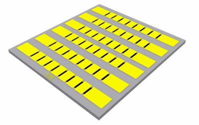
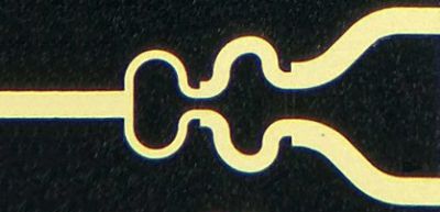
Supports the production of thin film integrated circuits that meet the customer's special pattern requirements on a number of ceramic substrates such as alumina, aluminum nitride, yttrium oxide, ferrite, and microwave substrates. * Fine metal strip width 0.02mm, metal strip * small pitch 0.02mm, precision ± 0.002mm; product * small appearance size 0.2mm × 0.2mm, precision ± 0.02mm; * small resistance 1Ω, * large resistance 50KΩ, accuracy 5% , 10%, special precision up to 0.5% (using laser trimming).
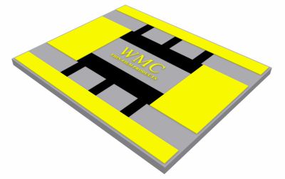
Supports fine lines, fine circuit fabrication, patterned ceramic side edges, metallization, side wall cladding, and double-sided patterned circuit fabrication.
Metalizations
WMC Sputtering is commonly used because the adhesion of deposited metals is excellent. The basic bondable metallization scheme for thin-film substrates contains TiW as the adhesion layer and Au as the conductor layer (TiW/Au).
square films are also available on single circuit designs.
Solderable metallization shemes are also available by adding Ni and/or Cu to these films (TiW/Au/Cu/Ni/Au). Bondable and solderable metallization schemes can be achieved on a single design. platinum can also be added as a solderable film when using high-temperature eutectics.
Metallization System | Application | component Attachment Method | Typical thickness range | Max. use temperature |
TiW/Au | Standard thin film metal system for conductors | Au/Sn,Au/Si,Au/Ge Eutectic;Epoxy | TaN:25–100Ω /sq TiW:500–800Å Au:0.5–5µm, typical =3µm | 425℃ |
TaN/TiW/Au | Standard thin film metal system for conductors with resistor layer | 380℃ | ||
TiW/Ni/Au | Conductor applications that require Pb/Sn soldering | Au/Sn,Au/Si,Au/Ge Eutectic;Pb/Sn;Epoxy | TaN:25–100Ω /sq TiW:500–800Å Ni:1000–10000Å Au:0.5–5µm, typical =3µm | 350℃ |
TaN/TiW/Ni/Au | Conductor with resistor layer applications that require Pb/Sn soldering | 350℃ | ||
TaN/TiW /Au/ Cu/Ni/Au | High current &low loss applications | Au/Sn,Au/Si,Au/Ge Eutectic;Pb/Sn | TaN:25–100Ω /sq TiW:500–800Å Ni:1000–10000Å Au:0.2–1µm Cu:0.5–12µm Ni:0.5–2µm | 350℃ |
Ti/Pt/Au/AuSn | brazing temperature Moderate , high strength, low viscosity
| Au/Sn | Ti:500–800Å Pt:0.2–1µm Au:0.2–1µm AuSn:1.5–10µm |
Contact information
Sales: sales@thinfilmcircuit.com
Engineer: vincent-wmc@foxmail.com
WeChat: thinfilmcircuit
Phone: +86 13061370991